How to enhance the effect of PCB antenna
As wireless technology continues to advance at a rapid pace, new methods must be found to keep up with the increasing demand for high-quality connectivity. One of the most important elements of any wireless device is the PCB antenna, which plays a crucial role in transmitting and receiving signals. However, even the most well-designed antenna can struggle to provide optimal performance under certain conditions. In this article, we will explore some methods for enhancing the effectiveness of a PCB antenna.
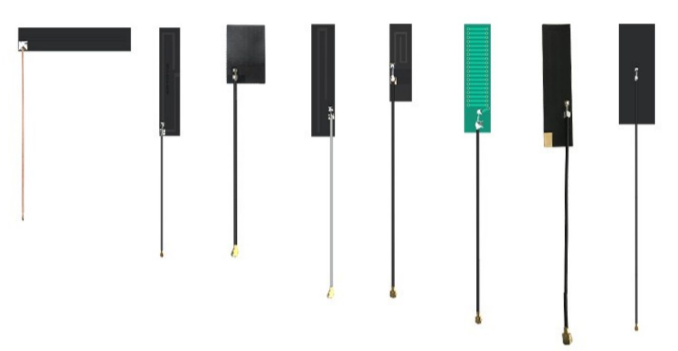
1. PCB antenna design
The design of the PCB antenna is one of the most critical factors that can influence its effectiveness. A well-designed antenna should be placed as close to the edge of the PCB as possible, as this can help to reduce interference from other components on the board. Additionally, the size and shape of the antenna should be optimized to match the frequency band of the wireless signal that is being used.
2. Ground plane
The ground plane is an essential element of any PCB antenna design. It helps to provide a stable reference point for the antenna and acts as a shield to reduce electromagnetic interference. An inadequate ground plane can cause a decrease in the antenna's effectiveness, leading to weaker signal strength.
3. Power delivery network
A stable and robust power delivery network is critical for optimal PCB antenna performance. The power supply voltage must be maintained within the design specifications to ensure that the antenna receives a sufficient power supply. Any disturbances in the power delivery network can lead to fluctuations in the antenna's impedance, resulting in unwanted signal reflections and a decrease in overall effectiveness.
4. Matching network
The matching network is responsible for adjusting the antenna's impedance to match that of the transmitter or receiver. An improper match can lead to a significant decrease in the antenna's effectiveness, resulting in weaker signal strength and lower data rates. A well-designed matching network can also help to reduce signal reflections and unwanted harmonics.
5. Shielding
Interference from external sources can cause a significant decrease in PCB antenna effectiveness. Shielding can be used to protect the antenna from external noise and allow it to function optimally. The use of copper shielding around the PCB and antenna can help to reduce unwanted electromagnetic interference and improve signal quality.
In conclusion, PCB antenna design plays an essential role in the overall performance of a wireless device. The effectiveness of the antenna can be enhanced through several different methods, including careful design, stable power delivery networks, optimized matching networks, and shielding. By taking these factors into account when designing a PCB antenna, it is possible to achieve optimal performance for any wireless application.
